Adder Circuit
Since the sampling circuit needs the voltage to be above 0V to be able to sample it and that the analog filtering circuit centers the voltage around 0V at the high-pass filtering step, the voltage needs to be offset to be entirely above 0V. This was not done on the prototype board and so an oscilloscope was needed to properly visualize the signal from the board.
Since the only amplification in the circuit is provided by the 1000x gain of the instrumentation amplifier, we expect the signals to be only in the microvolts range at this point. This means a 1.5 V offset is adequate for an ADC range of 0 – 3.3V. This offset is achieved via an ap amp adder circuit shown on figure 10. The effect of the adder circuit is shown in figure 11.
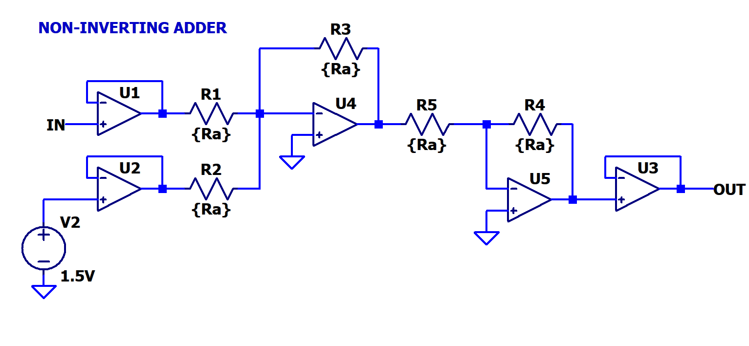 Figure 10: Adder Schematic
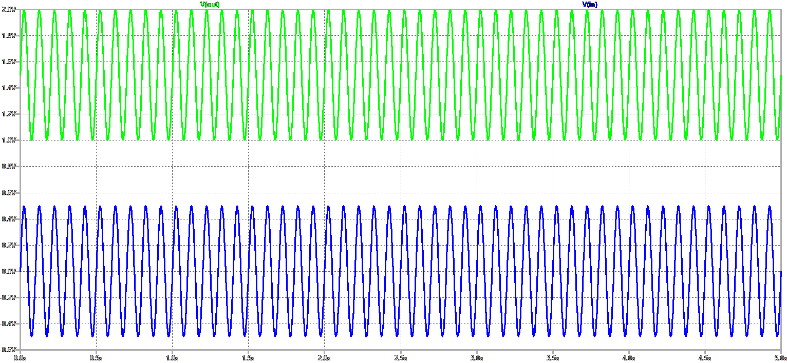 Figure 11: Adder Input (Blue), Adder Output (Green)